1.
建立一个没有input和一个output的电路。 该output应始终驱动 1(或逻辑高)。
module top_module( output high);

// 代码如下
    assign high = [修改此处];

endmodule
2.
构建一个没有输入和一个输出常量 0 的电路。
module top_module(
    output zero
);

// 这里添加模块主体代码

endmodule
3.
创建有一个input和一个output的模块,其行为类似于wire。
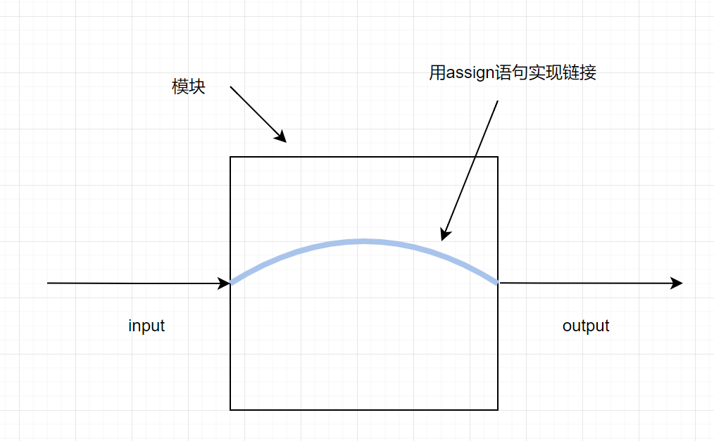
module top_module( input in, output out );
//使用assign语句实现

endmodule
4.
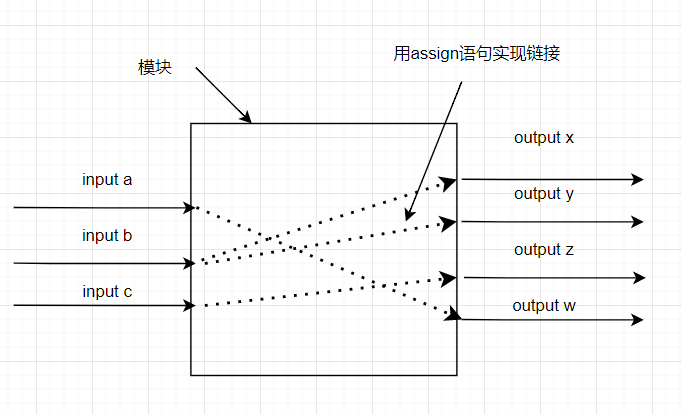
创建有 3 个input和 4 个output的模块,其行为类似于进行这些连线:
a -> w
b -> x
b -> y
c -> z
module top_module(
    input a,b,c,
    output w,x,y,z );

//使用assign语句实现

endmodule
5.
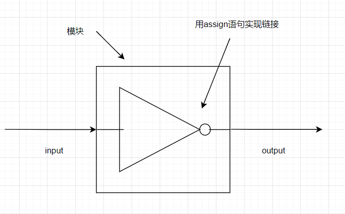
创建一个实现非门(NOT )的模块。
module top_module( input in, output out );
//使用assign语句实现
endmodule
6.
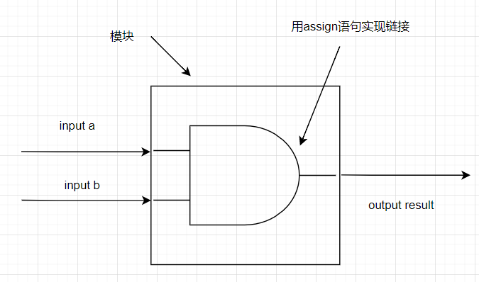
创建一个实现与门(AND )的模块。
module top_module(
    input a,
    input b,
    output result );

//使用assign语句实现

endmodule
7.
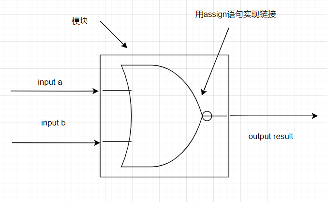
创建一个实现或非门(NOR)门的模块。 或非门(NOR)是输出反相的或(OR)门。 用 Verilog 编写时,NOR 函数需要两个运算符。
module top_module(
    input a,
    input b,
    output result );

//使用assign语句实现

endmodule
8.
创建一个实现同或门(XNOR )的模块。
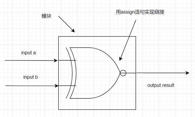
module top_module(
    input a,
    input b,
    output result );

//使用assign语句实现

endmodule
9.
学习wire 的声明使用:wire是将内部组件连接在一起。 当需要使用wire信号或变量时,应该在模块主体使用之前先进行声明(将来,可能遇到更多类型的信号和变量,它们也以相同的方式声明)。
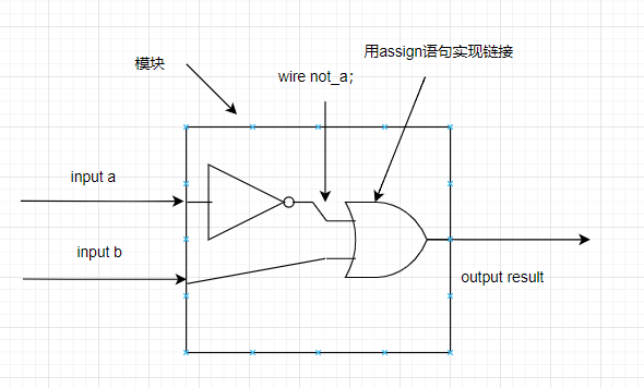
`default_nettype none
module top_module(
    input a,
    input b,
    output result
  );

wire not_a;

//使用assign语句实现

endmodule
10.
5451是具有4个与门和两个或非门的芯片。
创建一个与 5451芯片功能相同的模块。 它有 8个输入和 2 个输出。 可以选择使用assign语句来驱动每条输出线,或者可以选择声明wire 信号用作中间信号,其中每条内部线都由一个与门的输出驱动。
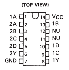
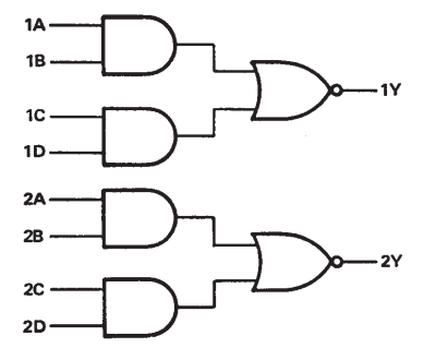
module top_module (
    input P1A,P1B,P1C,P1D,
    output P1Y,
    input P2A,P2B,P2C,P2D,
    output P2Y);


endmodule
以上问题的答案请参照相应视频: