上节内容讲解了同步DRAM的原理、分类及选型,本节内容将以美光的MT41J128M16HA-125为例着重讲解DDR3的内部结构以加深对DDR3的理解。
1. MT41J128M16HA-125 DDR3内部结构
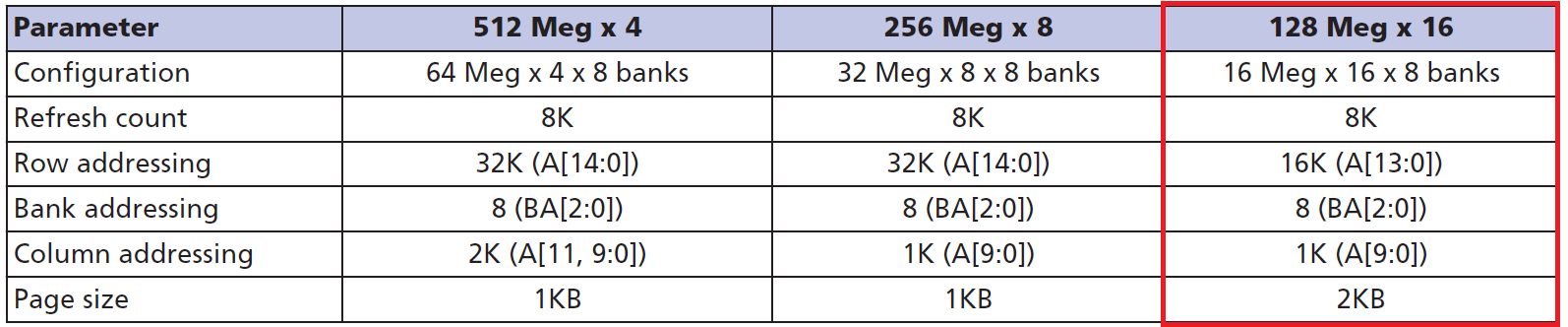
DDR3 寻址方式如表1,
表1
-
DDR3结构
DDR3是由行、列和BANK组成的立体结构,如图1所示。
(1)MT41J128M16HA-125的内部组织结构,由行与列组织一个BANK。其中每个BANK中包含16K(A[13:0])行,每行1K(A[9:0])列,每列对应16bits。
(2)由BA[2:0] 选择对应的BANK,共8个BANK。
(3)BANK选定后在行内操作,一行的容量为一个页面(Page ),对于MT41J128M16HA-125可寻址的列为1K(A[9:0]),每列为16bits。
-
DDR3内部为8倍数据预取或写入
以MT41J128M16HA-125为例,如图3所示,DDR3内部每次8倍的预读取,或8倍写入。对于读取数据,首先从存储阵列读取8列的内容,即16bit x 8的内容送到片内FIFO中,在FIFO的另一端以16bit的方式读出,这样在端口以时钟的上下边沿读取。虽然外部每4个时钟周期可以读8次(上升沿4次,下降沿4次),但在存储器内部的时钟频率仅为外部端口时钟的1/4。对于写数据,也是采用8倍写入的方式,原理与读取过程相似。这就是8n的读写过程。
-
端口数据交换
如图3,从内部单元以128位(8n)的方式读写到FIFO,每次读取需要4个CK。在从FIFO以16位(1n)的方式取出到数据IO,由于采用双边沿读写,因此每个数据交换只需要半个时钟周期。由于该部分结构都是由DDR内部实现,因此用户在使用时,往往并不关心多倍读取行为。只要确定端口的读写时序即可。
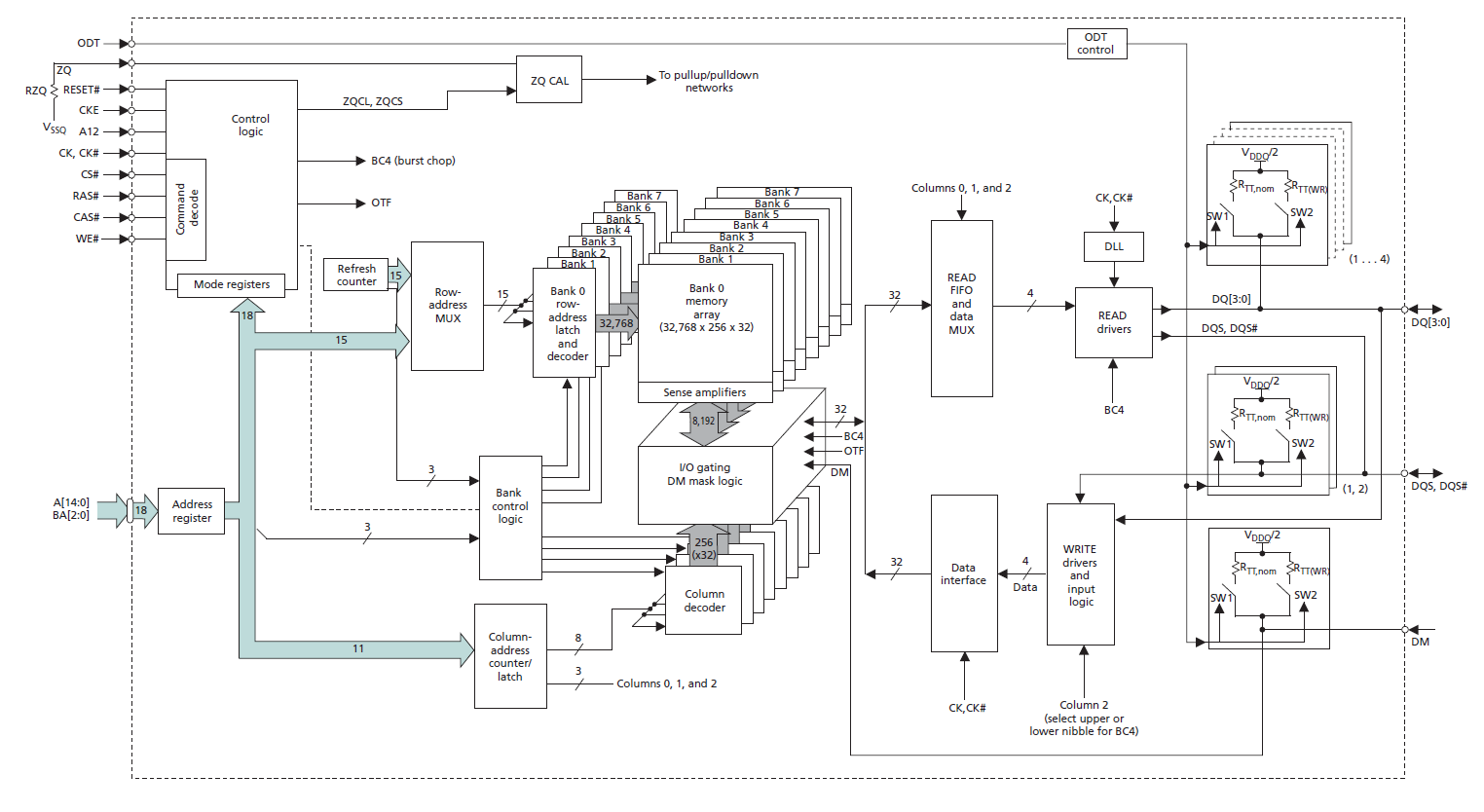
图1 DDR3 MT41J512M4DA-125内部结构
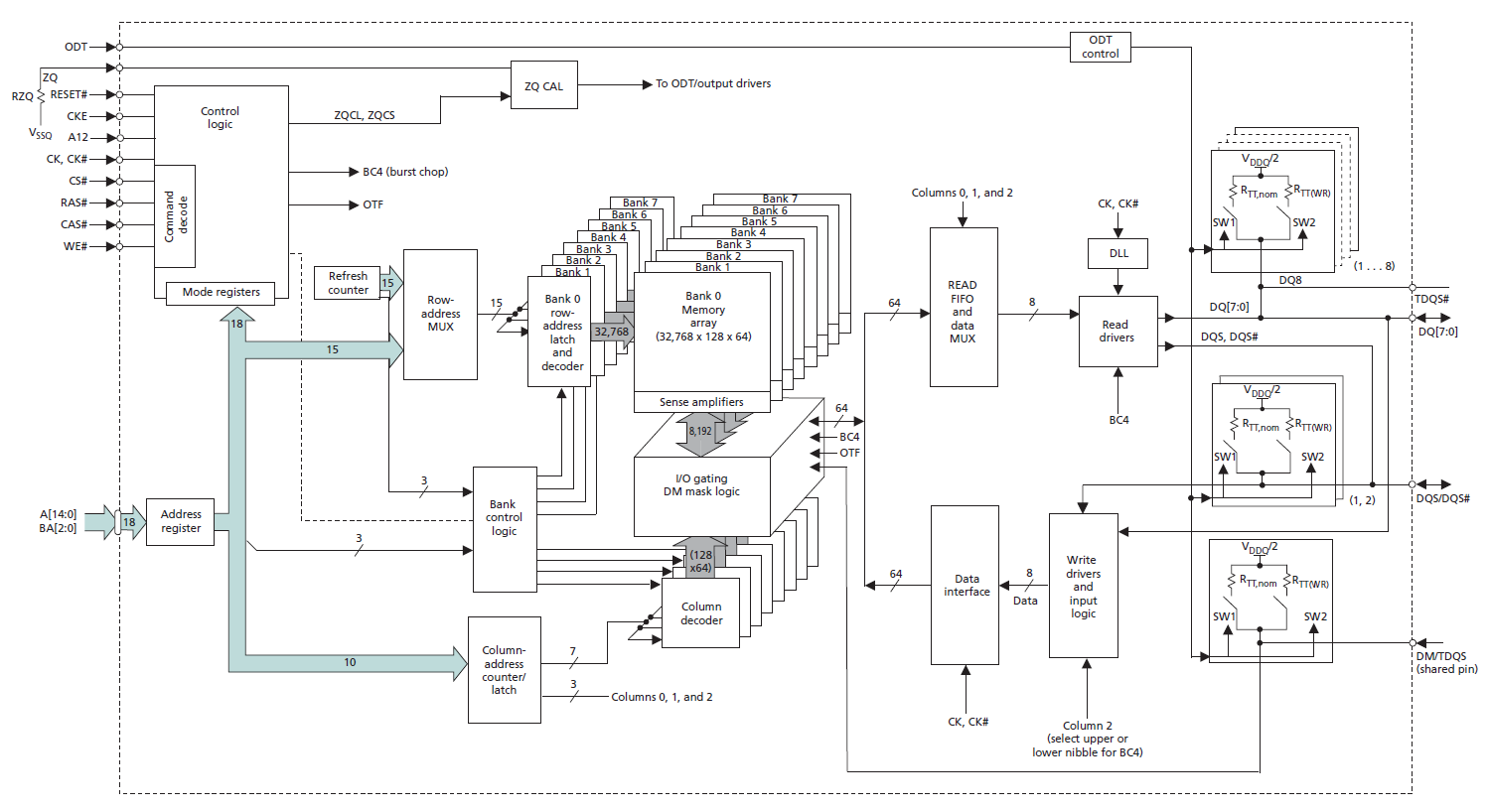
图2 MT41J256M8DA-125 DDR3内部结构示意图
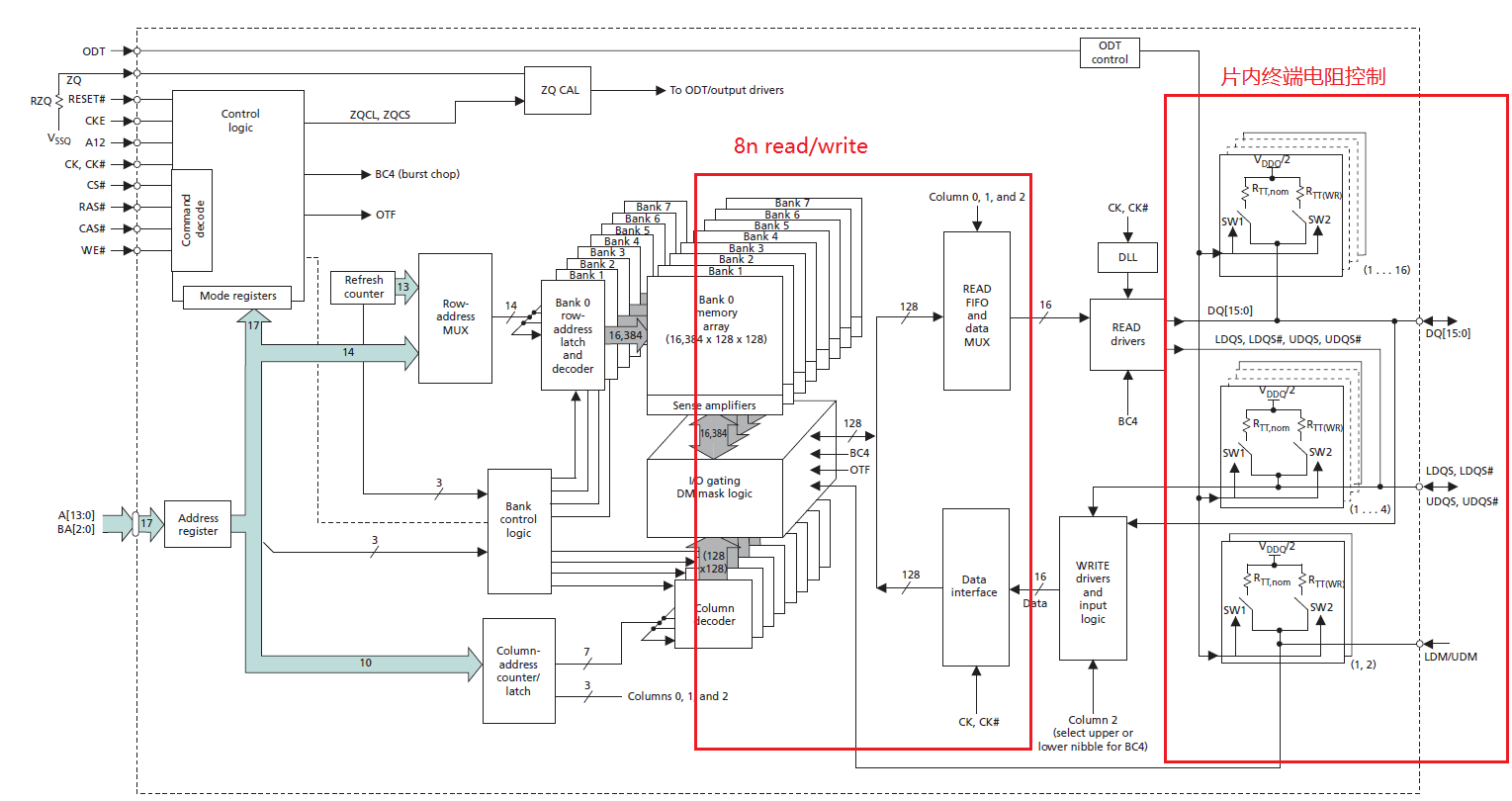
图3 MT41J128M16HA-125 DDR3内部结构示意图
2. MT41J128M16HA-125 DDR3接口描述
MT41J128M16HA-125 DDR3接口描述如表2所示
表2
| 名称(symbol) | 输入/输出
input/output |
description | 描述 |
| CS# | Input | Chip select:
CS# enables (registered LOW) and disables (registered HIGH) the command decoder. All commands are masked when CS# is registered HIGH. CS# provides for external rank selection on systems with multiple ranks. CS# is considered part of the command code. CS# is referenced to VREFCA. |
片选输入端:
在时钟的上升沿锁存过的值作为DDR3的命令的使能。 CS#为高时(锁存的CS#)屏蔽命令译码。 CS#提供外部不同RANK的选择。 CS#一般认为是DDR3命令的一个部分。 CS#的参考电压为VREFCA。 |
| LDM | Input | Input data mask:
LDM is a lower-byte, input mask signal for write data. Lower-byte input data is masked when LDM is sampled HIGH along with the input data during a write access. Although the LDM ball is input-only, the LDM loading is designed to match that of the DQ and DQS balls. LDM is referenced to VREFDQ. |
Lower (byte)data Mask
输入数据屏蔽: 低字节写数据屏蔽。当 LDM 采样到的值为高电平时在DDR3写数据时会屏蔽低字节的写,即低字节写无效。 时序上与DQ,DQS一致。 LDM 的参考电压为 VREFDQ。 |
| UDM | Input | Input data mask:
UDM is an upper-byte, input mask signal for write data. Upper-byte input data is masked when UDM is sampled HIGH along with that input data during a WRITE access. Although the UDM ball is input-only, the UDM loading is designed to match that of the DQ and DQS balls. UDM is referenced to VREFDQ. |
Upper (byte)data Mask
输入数据屏蔽: 高字节写数据屏蔽。当 UDM 采样到的值为高电平时在DDR3写数据时会屏蔽高字节的写,即高字节写无效。 时序上与DQ,DQS一致。 UDM 的参考电压为 VREFDQ。 |
| ODT | Input | On-die termination:
ODT enables (registered HIGH) and disables (registered LOW)termination resistance internal to the DDR3 SDRAM. When enabled in normal operation, ODT is only applied to each of the following balls: DQ[15:0], LDQS, LDQS#,UDQS, UDQS#, LDM, and UDM. The ODT input is ignored if disabled via the LOAD MODE command. ODT is referenced to VREFCA. |
片上终端电阻设定:
在时钟的上升沿锁存过的ODT的值为高电平将使能DDR3内部终端电阻。低电平时禁止片上终端电阻的接入。 见图3 当在正常操作下如果使能该信号,ODT仅对DQ[15:0],LDQS#,LDQS,UDQS #,UDQS,LDM,UDM 有效。 当通过载入模式命令(Load Mode)禁止ODT功能时,该信号被忽略。 ODT的参考电压为 VREFCA。 |
| RAS#,
CAS#, WE# |
Input | Command inputs:
RAS#, CAS#, and WE# (along with CS#) define the command being entered and are referenced to VREFCA. |
命令输入。与其他控制信号组合形成命令。
RAS#:行地址选通线(row address strobe), CAS# :列地址选通(column address strobe), WE# : 数据写使能 参考电压都为VREFCA。 |
| RESET# | Input | Reset: RESET# is an active LOW CMOS input referenced to VSS.
The RESET# input receiver is a CMOS input defined as a rail-to-rail signal with DC HIGH ≥ 0.8 × VDD and DC LOW ≤ 0.2 × VDDQ. RESET# assertion and de-assertion are asynchronous. |
复位信号,低电平有效
是异步信号。 电压范围: 高电平:DCHIGH ≥ 0.8 × VDD 低电平:DCLOW ≤ 0.2 × VDDQ |
| DQ[7:0] | I/O | Data input/output:
Lower byte of bidirectional data bus for the x16 configuration. DQ[7:0] are referenced to VREFDQ. |
低8为数据:
在16位配置中为低八位数据 参考电压为VREFDQ。 |
| DQ[15:8] | I/O | Data input/output:
Upper byte of bidirectional data bus for the x16 configuration. DQ[15:8] are referenced to VREFDQ. |
高8为数据:
在16位配置中为高八位数据 参考电压为VREFDQ |
| LDQS, LDQS# | I/O | Lower byte data strobe:
Output with read data. Edge-aligned with read data. Input with write data. Center-aligned to write data. |
差分信号对:
低八位数据选通, 读状态时输出,与读数据边沿对齐 写状态时输入,与数据中心对齐。 |
| UDQS, UDQS# | I/O | Upper byte data strobe:
Output with read data. Edge-aligned with read data. Input with write data. DQS is center-aligned to write data. |
差分信号对:
高八位数据选通, 读状态时输出,与读数据边沿对齐 写状态时输入,与数据中心对齐。 |
| VDD | Supply | Power supply: 1.5V ±0.075V | 芯片供电端:
电压范围1.5V ±0.075V |
| VDDQ | Supply | DQ power supply:
1.5V ±0.075V. Isolated on the device for improved noise immunity |
I/O的供电端:
电压范围1.5V ±0.075V。 与芯片的供电端隔离,提供抗噪效果。 |
| VREFCA | Supply | Reference voltage for control, command, and address:
VREFCA must be maintained at all times (including self refresh) for proper device operation |
参考电压:
是控制信号,地址,命令的参考电压,需全局维护(即使在自刷新阶段)。1.5V /1.35V的一半(0.75V/0.65V) |
| VREFDQ | Supply | Reference voltage for data: VREFDQ must be maintained at all times (excluding self refresh) for proper device operation. | 数据线的参考电压:
需全局维护(自刷新时除外) 1.5V/2或1.35V/2 |
| VSS | Supply | Ground | 芯片地 |
| VSSQ | Supply | DQ ground:
Isolated on the device for improved noise immunity. |
数据DQ的地,
与芯片地隔离,可以提高抗噪效果。 |
| ZQ | Reference | External reference ball for output drive calibration:
This ball is tied to external 240Ω resistor RZQ, which is tied to VSSQ. |
外部参考:
用来校准对外部驱动。一般通过240欧姆电阻RZQ接到VSSQ上。 |
本节内容出现了大量的概念和名词,后续课程将结合硬件设计,命令编程,DDR3控制器设计等内容再做详细解释。