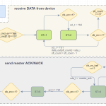
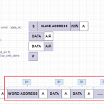
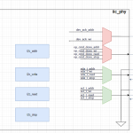
物理层芯片除了使用MII接口与MAC交换数据外,还有Phy芯片的管理接口用于管理PHY的行为。为了主机便于管理Phy层芯片的行为,MAC与Phy之间还有一个管理层接口,通常称为MDIO,是2线制的结构,与I2C有点类似。但是具体的读写行为不同。其中MDC为时钟信号,一般低于2.5Mhz。MDIO为双向数据信号,需要1.5K的上拉电阻来维持当空闲或反转时高电平的状态。
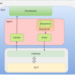
管理接口主要用来配置和管理Phy的命令和状态寄存器,Phy芯片常用的寄存器有32个。可以用来设置芯片的各种行为如复位,速度选择,流控等行为,以及自动协商后的状态等,硬件如图1
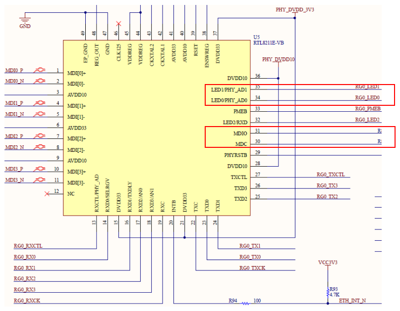
图1 MDIO接口
1 . 管理帧结构描述如表1
表1
| 命令/状态 | CMD/STATE | 值(value) | 行为(behavior) |
| 前置 | preamble
前导字 |
32个1
0xffff,32’hffff |
32 Contiguous Logical 1’s Sent by the MAC on MDIO,
along with 32 Corresponding Cycles on MDC. This provides synchronization for the PHY. MAC发送32个连续的1作为同步信号。 |
| 帧启动 | ST | 01 | Start of Frame 帧启动标志 |
| 读/写 | OP | 10 或 01 | Operation Code. Read: 10 Write: 01 |
| Phy地址 | PHYAD | 0-7 | PHY Address. Up to eight PHYs can be connected to one MAC.
This 3-bit field selects which PHY the frame is directed to. 由3个地址输入脚选择,最多总线上可以挂接8个Phy芯片, 实现芯片共享. 只有发送的地址数据与硬件设置的数据一致, 该芯片才会被选中 |
| 寄存器地址 | REGAD | 0-31 | Register Address.
This is a 5-bit field that sets which of the 32 registers of the PHY this operation refers to. PHY芯片内部总共32个寄存器,地址编码0-31 |
| 反转 | TA | Z0–读 写 | Turnaround. This is a 2-bit-ime spacing between the register
address and the data field of a frame to avoid contention during a read transaction. For a read transaction, both the STA and the PHY remain in a high-impedance state for the first bit time of the turnaround. The PHY drives a zero bit during the second bit time of the turnaround of a read transaction 读: MAC端的MDIO此刻起到帧结束一直为高阻态,PHY的MDIO 改为输出写:始终由MAC的MDIO控制,整个帧可以认为都是 写的过程。 |
| 数据 | DATA | These are the 16 bits of data. 16bits数据 | |
| 空闲 | IDLE | Idle Condition. Not truly part of the management frame.
This is a high impedance state. Electrically, the PHY’s pull-up resistor will pull the MDIO line to a logical ‘1’. 空闲可以认为不是帧的部分,空闲时MAC的MDIO为高阻, 由于有上拉电阻,总线上为高电平,Phy的MDIO为输入 |
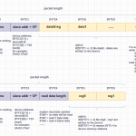
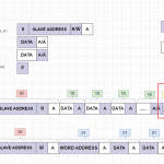
- MDIO读写时序
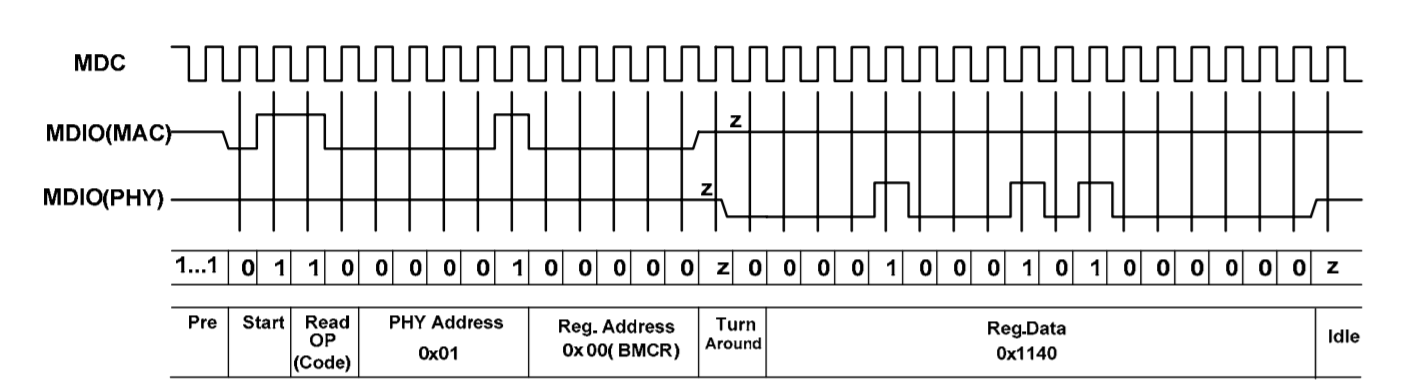
图2 读时序
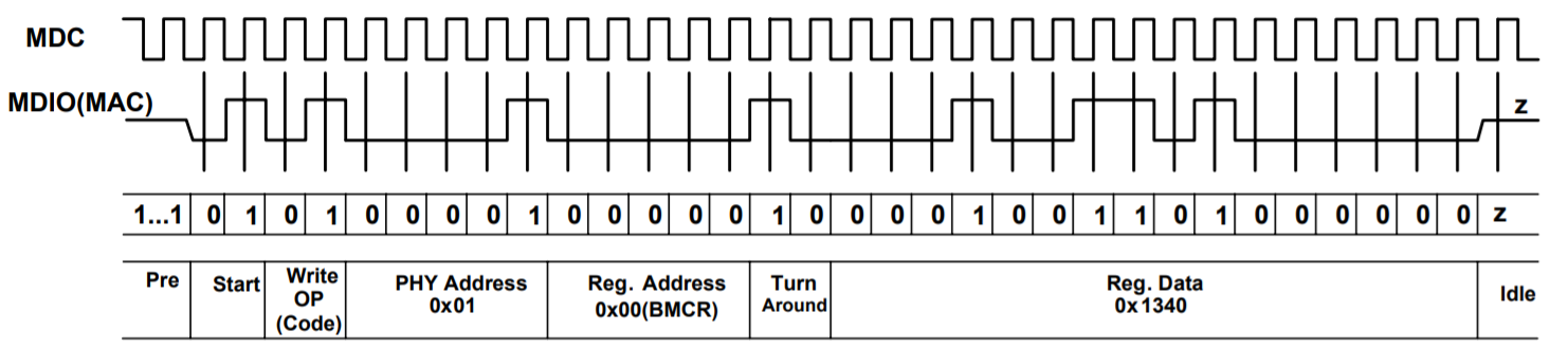
图3 写时序
在读写时序中用到PHY芯片的地址,由于MDIO是支持多芯片共享接口,因此在读写过程中利用地址选择不同芯片的读写,图1中的信号,LED0/PHY_AD0及LED1/PHY_AD1, 表示芯片硬件地址设置,已设置好的硬件地址应与MDIO读写地址匹配。