在完成DDR3控制器生成后,展开新生成ddr3_intf IP核并打开ddr3_intf.v文件,如图1所示。ddr3_intf是新生成的DDR3控制器的IP核。该IP核起到了在APP与DDR3芯片接口之间桥梁的作用。如果仅仅在FPGA上使用DDR3, 学会使用APP与DDR3控制器之间的接口和数据交互是必须要掌握的技能。当然该IP核源文件都可以阅读,是学习DDR3控制器开发的最好范例。
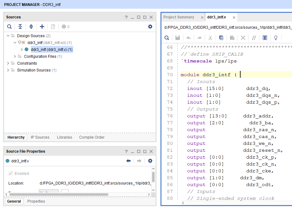
图1
在图1右边的文本编辑框中可以看到DDR3的输入输出接口,APP与DDR3控制器接口的框图见图-2。下面将以ddr3_intf IP 核为基础新建测试DDR3的应用与测试文件。操作步骤如下。
1. 新建测试文件新建测试文件ddr3_top.v.
- 将ddr3_intf.v的输入、输出部分复制到ddr3_top.v的输入输出部分,并在ddr3_top.v文件中例化ddr3_intf。
- 新建PLL(sys_pll)并例化。PLL的输入时钟为50MHz, 输出时钟clk_out1为100Mhz作为系统时钟;输出时钟clk_out2为DDR3控制器的参考时钟,时钟频率为200Mhz。如图2所示。
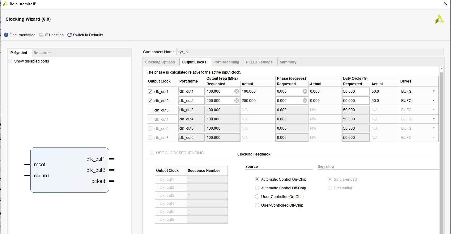
图2
2. ddr3_top.v的代码如下:
module DDR3_top
(

  input                             inclk,
    // Memory interface ports
  output    [13:0]                  ddr3_addr,      // output [13:0]		ddr3_addr
  output    [2:0]                   ddr3_ba,        // output [2:0]		ddr3_ba
  output                            ddr3_cas_n,     // output			ddr3_cas_n
  output                            ddr3_ck_n,      // output [0:0]		ddr3_ck_n
  output                            ddr3_ck_p,      // output [0:0]		ddr3_ck_p
  output                            ddr3_cke,       // output [0:0]		ddr3_cke
  output                            ddr3_ras_n,     // output			ddr3_ras_n
  output                            ddr3_reset_n,   // output			ddr3_reset_n
  output                            ddr3_we_n,      // output			ddr3_we_n
  inout     [15:0]                  ddr3_dq,        // inout [15:0]		ddr3_dq
  inout    [1:0]                    ddr3_dqs_n,     // inout [1:0]		ddr3_dqs_n
  inout    [1:0]                    ddr3_dqs_p,     // inout [1:0]		ddr3_dqs_p


  output    [1:0]                   ddr3_dm,                    // output [1:0]		ddr3_dm
  output    [0:0]                   ddr3_odt


);


  wire                          init_calib_complete ; // output			init_calib_complete

  wire      [26:0]              app_addr;           // input [26:0]		app_addr
  wire      [2:0]               app_cmd;             // input [2:0]		app_cmd
  wire                          app_en;           // input				app_en
  wire                          app_rdy;            // output			app_rdy

  wire      [127:0]             app_wdf_data;        // input [127:0]		app_wdf_data
  wire                          app_wdf_end;        // input				app_wdf_end
  wire                          app_wdf_wren;       // input				app_wdf_wren
  wire                          app_wdf_rdy ;      // output			app_wdf_rdy
   wire     [15:0]              app_wdf_mask;     // input [15:0]		app_wdf_mask

  wire      [127:0]             app_rd_data;        // output [127:0]		app_rd_data
  wire                          app_rd_data_end;    // output			app_rd_data_end
  wire                          app_rd_data_valid ;  // output			app_rd_data_valid


 // reg                               app_sr_req       ;       // input			app_sr_req
 // reg                               app_ref_req    ;      // input			app_ref_req
 // reg                               app_zq_req    ;      // input			app_zq_req
//  wire                              app_sr_active  ;    // output			app_sr_active
//  wire                              app_ref_ack;     // output			app_ref_ack
//  wire                              app_zq_ack;      // output			app_zq_ack
  wire                              ui_clk   ;           // output			ui_clk
  wire                              ui_clk_sync_rst; // output			ui_clk_sync_rst

    // System Clock Ports
  wire                              sys_clk;  //4?1  100M
    // Reference Clock Ports
  wire                              clk_ref ;//200M
  wire                              pll_locked;

  wire          nsys_rst=pll_locked;

sys_pll  sys_pll_inst
 (
  // Clock out ports
.clk_out1   (sys_clk),//ratio 2:1 200M,4:1 ---100Mhz
.clk_out2   (clk_ref),//200M
  // Status and control signals
.reset      (1'b0),
.locked     (pll_locked),
 // Clock in ports
.clk_in1    (inclk)   //50M
 );


 ddr3_intf u_ddr3_intf (

    // Memory interface ports
    .ddr3_addr                      (ddr3_addr),  // output [13:0]		ddr3_addr
    .ddr3_ba                        (ddr3_ba),  // output [2:0]		ddr3_ba
    .ddr3_cas_n                     (ddr3_cas_n),  // output			ddr3_cas_n
    .ddr3_ck_n                      (ddr3_ck_n),  // output [0:0]		ddr3_ck_n
    .ddr3_ck_p                      (ddr3_ck_p),  // output [0:0]		ddr3_ck_p
    .ddr3_cke                       (ddr3_cke),  // output [0:0]		ddr3_cke
    .ddr3_ras_n                     (ddr3_ras_n),  // output			ddr3_ras_n
    .ddr3_reset_n                   (ddr3_reset_n),  // output			ddr3_reset_n
    .ddr3_we_n                      (ddr3_we_n),  // output			ddr3_we_n
    .ddr3_dq                        (ddr3_dq),  // inout [15:0]		ddr3_dq
    .ddr3_dqs_n                     (ddr3_dqs_n),  // inout [1:0]		ddr3_dqs_n
    .ddr3_dqs_p                     (ddr3_dqs_p),  // inout [1:0]		ddr3_dqs_p


    .ddr3_dm                        (ddr3_dm),  // output [1:0]		ddr3_dm
    .ddr3_odt                       (ddr3_odt),  // output [0:0]		ddr3_odt

    // Application interface ports
    .init_calib_complete            (init_calib_complete),  // output			init_calib_complete

    .app_addr                       (app_addr),  // input [27:0]		app_addr
    .app_cmd                        (app_cmd),  // input [2:0]		app_cmd
    .app_en                         (app_en),  // input				app_en
    .app_rdy                        (app_rdy),  // output			app_rdy


    .app_wdf_data                   (app_wdf_data),  // input [127:0]		app_wdf_data
    .app_wdf_end                    (app_wdf_end),  // input				app_wdf_end
    .app_wdf_wren                   (app_wdf_wren),  // input				app_wdf_wren
    .app_wdf_rdy                    (app_wdf_rdy),  // output			app_wdf_rdy
    .app_wdf_mask                   (app_wdf_mask),  // input [15:0]		app_wdf_mask

    .app_rd_data                    (app_rd_data),  // output [127:0]		app_rd_data
    .app_rd_data_end                (app_rd_data_end),  // output			app_rd_data_end
    .app_rd_data_valid              (app_rd_data_valid),  // output			app_rd_data_valid


    .app_sr_req                     (1'b0),  // input			app_sr_req
    .app_ref_req                    (1'b0),  // input			app_ref_req
    .app_zq_req                     (1'b0),  // input			app_zq_req
    .app_sr_active                  (),  // output			app_sr_active
    .app_ref_ack                    (),  // output			app_ref_ack, refresh
    .app_zq_ack                     (),  // output			app_zq_ack

    .ui_clk                         (ui_clk),  // output			ui_clk
    .ui_clk_sync_rst                (ui_clk_sync_rst),  // output			ui_clk_sync_rst

    // System Clock Ports
    .sys_clk_i                       (sys_clk),
    // Reference Clock Ports
    .clk_ref_i                      (clk_ref),// reference
    .sys_rst                        (nsys_rst) // input sys_rst
    );

  //application
ddr_rd_wr  ddr_rd_wr_inst
(
.app_addr           (app_addr),
.app_cmd            (app_cmd),
.app_en             (app_en),
.app_rdy            (app_rdy),

.app_wdf_data       (app_wdf_data),
.app_wdf_end        (app_wdf_end),
.app_wdf_wren       (app_wdf_wren),
.app_wdf_rdy        (app_wdf_rdy),
.app_wdf_mask       (app_wdf_mask),

.app_rd_data        (app_rd_data),
.app_rd_data_end    (app_rd_data_end),
.app_rd_data_valid  (app_rd_data_valid),

.clk                (ui_clk),   //100M
.rst_n              (!ui_clk_sync_rst),
.error_flag         (error_flag),
.end_flag           (end_flag)

);

endmodule
ddr3_top.v的文件中 ddr_rd_wr例化部分是新建文件ddr_rd_wr.v,该文件利用ddr_intf接口进行DDR3存储器读写测试, 后面的章节会详细介绍.
3. DDR 控制器接口描述:
表1
| Signal name | Direction | Description | 描述 |
| app_addr[ADDR_WIDTH – 1:0] | input | This input indicates the address for
the current request. |
当前请求地址,[ROW+BA+COL) |
| app_cmd[2:0] | input | This input selects the command for
the current request. |
当前请求命令,000–写,001–读 |
| app_en | input | This is the active-High strobe for the
app_addr[], app_cmd[2:0], app_sz, and app_hi_pri inputs. |
高电平有效的选通信号,使能APP的地址,命令等 |
| app_rdy | output | This output indicates that the UI is ready
to accept commands.If the signal is deasserted when app_en is enabled, the current app_cmd and app_addr must be retried until app_rdy is asserted. |
指示当前的UI准备好接收新命令,如果在app_en使能后该信号撤销,命令及地址需重新发送 |
| app_hi_pri | input | This active-High input elevates the priority
of the current request. |
提升当前命令的优先级,常规设计中一般不使用 |
| app_rd_data
[APP_DATA_WIDTH – 1:0] |
output | This provides the output data from read
commands. |
读到的数据 |
| app_rd_data_end | output | This active-High output indicates that the
current clock cycle is the last cycle of output data on app_rd_data[]. This is valid only when app_rd_data_valid is active-High.zai |
当前时钟的数据为最后一笔数据,只有在app_rd_data_valid 为高电平时才有效 |
| app_rd_data_valid | output | This active-High output indicates
that app_rd_data[] is valid. |
高电平指示app_rd_data[] 有效 |
| app_sz | input | This input is reserved and
should be tied to 0. |
保留,输入0 |
表2
| Signal name | Direction | Description | 描述 |
| app_wdf_data
[APP_DATA_WIDTH – 1:0] |
input | This provides the data for write
commands. |
写命令之后跟的写数据 |
| app_wdf_end | input | This active-High input indicates that
the current clock cycle is the last cycle of input data on app_wdf_data[]. |
当前时钟的写数据为最后写命令的最后一笔数据. 是写数据与auto_precharge的组合 |
| app_wdf_mask
[APP_MASK_WIDTH – 1:0] |
input | This provides the mask for
app_wdf_data[]. |
每个字节对应的屏蔽位,每个bit对于数据的一个字节,高电平有效. |
| app_wdf_rdy | output | This output indicates that the write data
FIFO is ready to receive data. Write data is accepted when app_wdf_rdy = 1’b1 and app_wdf_wren = 1’b1. |
指示写数据缓冲区FIFO可以接收新数据,写数据在
app_wdf_rdy = 1’b1与app_wdf_wren = 1’b1.都有效是写数据才会被接受 |
| app_wdf_wren | input | This is the active-High strobe for
app_wdf_data[]. |
写使能
写数据在app_wdf_rdy = 1’b1与app_wdf_wren = 1’b1.都有效是写数据才会被接受 |
| app_correct_en_i | input | When asserted, this active-High signal
corrects single bit data errors. This input is valid only when ECC is enabled in the GUI. In the example design, this signal is always tied to 1. |
在ECC有效的情况下,如果该位有效可以纠正一位错误 |
| app_sr_req | input | This input is reserved and should be
tied to 0. |
保留,接0 |
| app_sr_active | output | This output is reserved. | 保留 |
| app_ref_req | input | This active-High input requests that
a refresh command be issued to the DRAM. |
请求刷新命令 |
表3
| Signal name | Direction | Description | 描述 |
| app_ref_ack | Output | This active-High output indicates that the
Memory Controller has sent the requested refresh command to the PHY interface |
高电平指示刷新命令已经送到DDR接口 |
| app_zq_req | Input | This active-High input requests that a ZQ
calibration command be issued to the DRAM. |
数据端口校准命令.
可以由应用程序发起 |
| ui_clk | Output | This UI clock must be a half or quarter of the
DRAM clock. |
用户时钟,是DDR控制器提供给APP的时钟,与DDR控制器的地址,数据及控制信号同步.
必须是一半(1/2)或1/4 的DDR时钟频率 |
| init_calib_complete | Output | PHY asserts init_calib_complete when
calibration is finished. |
校准完成后输出高电平.
可以用来指示DDR控制器的读写操作可以开始. |
| app_ecc_multiple_err[7:0] | Output | This signal is applicable when ECC is enabled
and is valid along with app_rd_data_valid. The app_ecc_multiple_err[3:0] signal is non-zero if the read data from the external memory has two bit errors per beat of the read burst. The SECDED algorithm does not correct the corresponding read data and puts a non-zero value on this signal to notify the corrupted read data at the UI. |
只有在ECC使能的情况下有效,在每个突发读时app_ecc_multiple_err[3:0]在检查到数据有2位错时输出非零值。如果采用SECDED算法,该机制并不纠错,只是输出一个非零值。 |
| ui_clk_sync_rst | Output | This is the active-High UI reset. | 高电平有效的UI复位信号 |
| app_ecc_single_err[7:0] | Output | This signal is applicable when ECC is enabled
and is valid along with app_rd_data_vali. The app_ecc_single_err signal is non-zero if the read data from the external memory has a single bit error per beat of the read burst. |
只有在ECC使能的情况下有效,在每个突发读时app_ecc_multiple_err[3:0]在检查到数据有1位错时输出非零值。如果采用SECDED算法,该机制并不纠错,只是输出一个非零值。 |
DDR3控制器的主要接口分为3组,分别地址命令的写入, 读数据命令,写数据命令. 注意这些接口主要用于FPGA内部应用程序与DDR控制器的接口,而不是FPGA应用程序与DDR3芯片的直接接口.其它的接口有refresh和ZQ calibration接口也是需要APP通过DDR控制器发给DDR3 SDRAM芯片. 通过以上接口可以实现APP与DDR_CTRL 中FIFO的交互. DDR控制器控制FIFO的另一端与DDR3芯片交互.
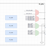
FPGA内APP与DDR控制器接口示意图,如图2,
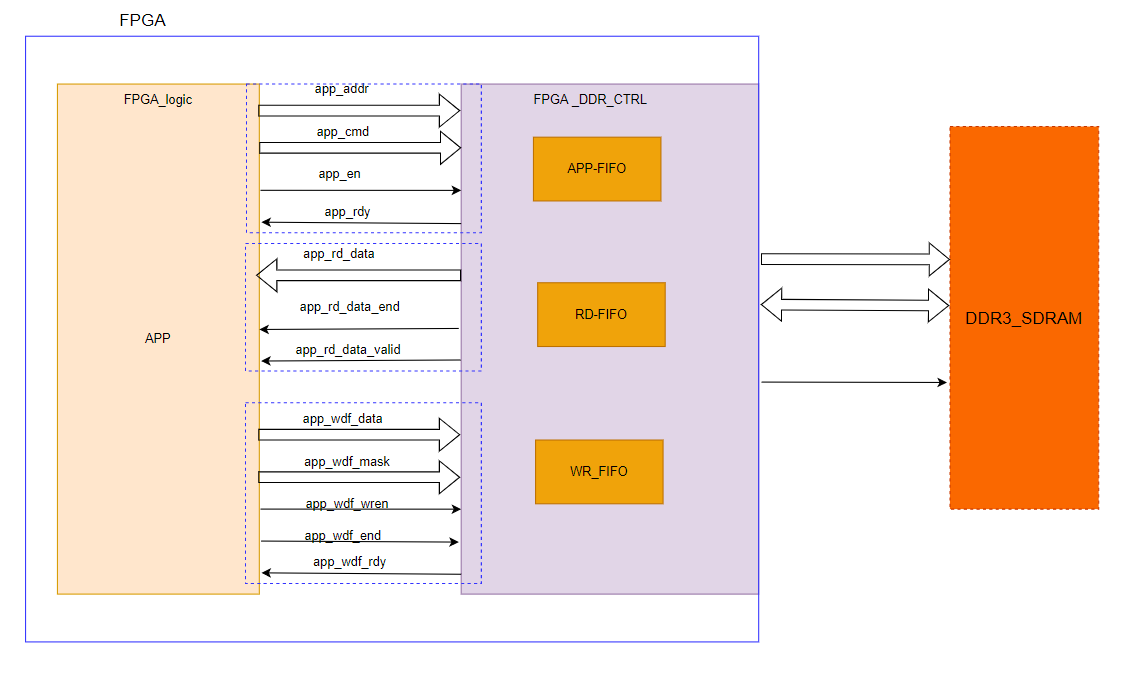
图2 FPGA_APP 与DDR控制器主要接口示意图
总结:在以生成的DDR控制器的基础上,学习APP-DDR Control之间的接口,例化DDR3控制器,并插入读写模块形成完整的应用程序。更过的内容请阅读后续文章。

老师好,在学习中遇到一些问题,请老师解答:
1、使用FPGA内部PLL生成的200M时钟作为ddr控制器的参考时钟,请问这里的参考时钟的频率是根据什么确定的呢?ddr控制器参考时钟必须使用200M时钟吗?
2、200M ddr控制器参考时钟,具体是用在哪里呢?有哪些具体作用呢?
使用FPGA内部PLL生成的200M时钟作为ddr控制器的参考时钟,请问这里的参考时钟的频率是根据什么确定的呢?
ddr控制器参考时钟必须使用200M时钟吗?
A:参考时钟200M 是由于artix芯片所决定的, 是必须的。 原因:这个参考时钟用来做MIG IP 的 IO delay 的,aritx芯片要求必须使用200M时钟,作为IO delay的。 高端的芯片有使用300M, 400M的。
200M ddr控制器参考时钟,具体是用在哪里呢?有哪些具体作用呢?
A:在 Ip 核中的mig_7series_v4_1_iodelay_ctrl.v 文件中的 340 – 357 行的位置,用来控制原语 IDELAYCTRL的。